The following explains the design of a control circuit for the TFT-LCD module LQ043T3DX02 Sharp, best known as the display used in the PlayStation Portable (PSP). It has a 480x272 resolution capable of displaying up to 16 million colors through a data bus 24-bit RGB backlight built. This display will be controlled through a spartan 3E FPGA verilog programmed to display three vertical bands of different colors, this didactic purposes, both the hardware design and the code in verilog. Although they work fine as long as practicable to improve, in fact the reader is invited to do so and leave your comments.
 |
| TFT_LCD LQ043T3DX02 Sharp |
CIRCUIT DESIGN
We start with the design of the hardware required for the LCD, then the first thing is to ensure the display voltage levels are compatible with the FPGA, for this we must rely on the following tables, obtained from data sheets of both devices.
 |
| Voltage levels of LCD |
 |
| Voltage levels of FPGA |
The communication is done from the FPGA to the LCD, then we are interested in observing the values of Vih and Vil of the LCD and Voh, Vol of the FPGA (LVCMOS25).
Then we can draw the following tables, the LCD requires between 0 and 0.5 V for reading a logical "0" and between 2 and 2.5V for a logical "1", in this case the FPGA occurs between 0 and 0.4 V maximum to a logical "0" and between 2.1 and 2.5 for a logical "1" in the same way the current input to the logic levels LCD Ioh, Iol is 4uA while in the fpga output currents of the pins are on the order of mA and check that the FPGA can directly drive the LCD and do not need any conditioning circuit.
Once verified this parameters, we start build a block diagram of the circuit.

SUPPLY CIRCUIT
This circuit should produce the necessary voltages for the LCD and the backlight. based on the data sheet, we observe that requires 2.5V and 5V where the maximum current for source is 3mA for the 2.5V and 5V for the 18mA.
The backlight consists of seven LEDs connected in series, with a maximum of 20 mA.
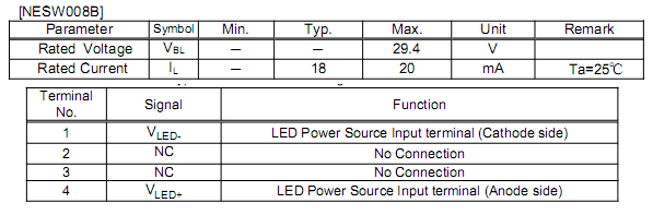 |
| Levels max of voltages and currents on the LCD |
The timing of start sequence shown below:
 |
| Start sequence of LCD |
The most critical requirement is that you should never supply AVDD before VCC.
DATA BUS This is an interface between the FPGA and display, via a ribbon cable to communicate the pins of the connector NEXYS 2 and 40-pin FPC of the screen.
ELECTION OF COMPONENTS The circuit is supply from a DC power supply with input voltage 100-240VAC, output 5VDC 100mA, which are inexpensive and readily available.
 |
| DC power supply |
This adapter provides 5VDC voltage required by the display.
For 2.5VDC and variable current source from 0 to 20mA LM317 regulator was chosen for its versatility, good accuracy, low cost and easy to achieve, some would prefer a low-dropout regulator, or with better electrical characteristics, is left to judgment of the reader any election that meets the specifications of the circuit.
Once collected the data we proceed to design the circuit schematic:
 |
| Schematic circuit |
In the schematic circuit IC1 configured as a voltage source variable with 5VDC input, 2.5VDC produced by programming the potentiometer R14.
The regulator IC8 is configured as variable current source which supply the backlight:

The previous scheme was modified to ensure that not more than 20mA, placing a fixed resistance of 68 ohms in series with the potentiometer (R4 and R17 see diagram) so that the maximum output current is Iout = 1.25/68 => Iout = 18.3mA (when R17 = 0) with a power of P = 1.25 * 20mA => P = 25 mW was obtained commercially 1/4W and not exceed the maximum allowed for the backlight.
The potentiometer 1k was chosen so that the minimum current (when R4 + R17) is 1.17mA.
DATA BUS The display has 40 pins in total of which 20 will be connected to the FPGA, the pinout is: will use 5 bits for red (R), 6 bits for green (G), 5 bits for blue (B) and 4 pins are for control, CK, DISP, Hsync, Vsync.
 |
| Pin info of LCD |
Each pin of the LCD was assigned one corresponding to the FPGA via the expansion port of the board NEXYS 2 by Hirose connector whose pin assignment is as follows:
 |
| pin info Nexys 2 |
 |
| Nexys 2 Board |
For this project we used an extra board that makes the interface between the connector Hirose FX2 connector and a standard ribbon cable:
 |
| FX2 interface |

| FPGA GPIO | NEXYS GPIO | LCD PIN | COMMENT |
| A4 | IO2 | R3 | RED |
| C4 | IO4 | R4 | RED |
| D5 | IO6 | R5 | RED |
| F7 | IO8 | R6 | RED |
| A6 | IO10 | R7 | RED (MSB) |
| F8 | IO12 | G2 | GREEN |
| E8 | IO14 | G3 | GREEN |
| C9 | IO16 | G4 | GREEN |
| G9 | IO18 | G5 | GREEN |
| D10 | IO20 | G6 | GREEN |
| B10 | IO22 | G7 | GREEN (MSB) |
| D11 | IO24 | B3 | BLUE |
| B11 | IO26 | B4 | BLUE |
| E11 | IO28 | B5 | BLUE |
| E12 | IO30 | B6 | BLUE |
| A13 | IO32 | B7 | BLUE (MSB) |
| E13 | IO34 | CK | CLOCK |
| C14 | IO36 | DISP | DISPLAY ON/OFF |
| B14 | IO38 | HSYNC | HORIZONTAL SYNC |
| B16 | IO40 | VSYNC | VERTICAL SYNC |
Finally designing a dual-layer PCB with surface mount components:
 |
| Bottom |
 |
| Top |
 |
| Silkscreen |
 |
| PCB |
The aim of the circuit is three columns show the colors red, blue, green on the display, so the circuit in the FPGA must:
1. Produce the start sequence, display enable and the LCD clock.
2. Generating synchronizing signals.
3. Send color data according to the position of the pixel.
To meet these criteria are designed the following flowchart:

1. START SEQUENCE AND CLOCK: First we review the sequence of supply voltages and signals. CK, Hsync, Vsync, DISP.


Based on the above information is created the next machine control
 |
| machine of control |
Wherein the enable signal SYNC synchronization module, AVDD supply voltage corresponds to the display enable signal and reading data.
The module is also responsible for activating the synchronization module.
We then the control module in verilog as follows:
VERILOG MODULE FOR START ON SEQUENCE
The module is also responsible for activating the synchronization module.
We then the control module in verilog as follows:
VERILOG MODULE FOR START ON SEQUENCE
module Control(Enable, en, rst, clk_lcd, off_lcd, en_sync, reset,
AVDD);
input wire Enable, rst, clk_lcd, off_lcd;
output reg en_sync, en, reset, AVDD;
reg [3:0] S;
reg [3:0] SS;
parameter [3:0]init=0;
parameter [3:0]Espera=1;
parameter [3:0]LCD_ON1=2;
parameter [3:0]LCD_ON2=3;
parameter [3:0]LCD_OFF1=4;
parameter [3:0]LCD_OFF2=5;
//Next state logic
always @(S or Enable or rst or off_lcd)
case (S)
init: if(Enable) SS=Espera; else SS=init;
Espera: if(Enable) SS=LCD_ON1; else SS=init;
LCD_ON1: SS=LCD_ON2;
LCD_ON2: if(Enable) SS=LCD_ON2; else SS=LCD_OFF1;
LCD_OFF1: if(off_lcd) SS=LCD_OFF2; else SS=LCD_OFF1;
LCD_OFF2: if(Enable) SS=init; else SS=LCD_OFF2;
default: SS=init;
endcase
//State memory
always @(posedge clk_lcd)
if(rst) S=init;
else S=SS;
//Output logic
always @(S)
case (S)
init: begin en_sync=0; AVDD=1; reset=1; en=0; end
Espera: begin en_sync=0; AVDD=1; reset=0; en=0; end
LCD_ON1: begin en_sync=1; AVDD=1; reset=0; en=1; end
LCD_ON2: begin en_sync=1; AVDD=1; reset=0; en=1; end
LCD_OFF1: begin en_sync=1; AVDD=1; reset=0; en=0; end
LCD_OFF2: begin en_sync=0; AVDD=0; reset=0; en=0; end
default: begin en_sync=0; AVDD=1; reset=1; en=0; end
endcase
endmodule
The display operates at frequency of 9 MHz, so we produce that frequency from the clock of the FPGA, in our case we use a Spartan 3E at 50Mhz, so for simplicity, we have two modules, the first is responsible for multiplying the frequency by two, the second is for dividing the frequency and obtain 9 MHz:
VERILOG MODULE TO MULTIPLY THE INPUT FRECUENCY BY A FACTOR OF TWO
module clk100(CLKIN_IN, CLKIN_IBUFG_OUT, CLK0_OUT,
CLK2X_OUT);
input CLKIN_IN;
output CLKIN_IBUFG_OUT;
output CLK0_OUT;
output CLK2X_OUT;
wire CLKFB_IN;
wire CLKIN_IBUFG;
wire CLK0_BUF;
wire CLK2X_BUF;
wire GND_BIT;
assign GND_BIT = 0;
assign CLKIN_IBUFG_OUT = CLKIN_IBUFG;
assign CLK0_OUT = CLKFB_IN;
IBUFG CLKIN_IBUFG_INST (.I(CLKIN_IN),
.O(CLKIN_IBUFG));
BUFG CLK0_BUFG_INST (.I(CLK0_BUF),
.O(CLKFB_IN));
BUFG CLK2X_BUFG_INST (.I(CLK2X_BUF),
.O(CLK2X_OUT));
DCM DCM_INST (.CLKFB(CLKFB_IN),
.CLKIN(CLKIN_IBUFG),
.DSSEN(GND_BIT),
.PSCLK(GND_BIT),
.PSEN(GND_BIT),
.PSINCDEC(GND_BIT),
.RST(GND_BIT),
.CLKDV(),
.CLKFX(),
.CLKFX180(),
.CLK0(CLK0_BUF),
.CLK2X(CLK2X_BUF),
.CLK2X180(),
.CLK90(),
.CLK180(),
.CLK270(),
.LOCKED(),
.PSDONE(),
.STATUS());
defparam DCM_INST.CLK_FEEDBACK = "1X";
defparam DCM_INST.CLKDV_DIVIDE = 2.0;
defparam DCM_INST.CLKFX_DIVIDE = 1;
defparam DCM_INST.CLKFX_MULTIPLY = 4;
defparam DCM_INST.CLKIN_DIVIDE_BY_2 = "FALSE";
defparam DCM_INST.CLKIN_PERIOD = 20.000;
defparam DCM_INST.CLKOUT_PHASE_SHIFT = "NONE";
defparam DCM_INST.DESKEW_ADJUST = "SYSTEM_SYNCHRONOUS";
defparam DCM_INST.DFS_FREQUENCY_MODE = "LOW";
defparam DCM_INST.DLL_FREQUENCY_MODE = "LOW";
defparam DCM_INST.DUTY_CYCLE_CORRECTION = "TRUE";
defparam DCM_INST.FACTORY_JF = 16'h8080;
defparam DCM_INST.PHASE_SHIFT = 0;
defparam DCM_INST.STARTUP_WAIT = "FALSE";
endmodule
Then we proceed to design the module to divide the frequency to get exactly 9MHz. because the module can only divide by integer factors, then it was very difficult to get them from a frequency of 50Mhz.
VERILOG MODULE TO DIVIDE THE INPUT FREQUENCY AND GET 9 MHz
module divisor_DISP(Clk, reset, clock_lcd);
input Clk, reset;
output reg clock_lcd;
parameter Divisor_DISP = 6;
parameter Bitcnt_DISP = 3;
reg [Bitcnt_DISP:0] Cnt_DISP;
always @ (posedge Clk or posedge reset)
begin
if (reset)
begin
clock_lcd<=0;
Cnt_DISP<=0;
end
else
begin
if(Cnt_DISP<(Divisor_DISP))
begin
clock_lcd<=1;
Cnt_DISP<=Cnt_DISP+1;
end
else
begin
if(Cnt_DISP<(Divisor_DISP)*2)
begin
clock_lcd<=0;
Cnt_DISP<=Cnt_DISP+1;
end
else
begin
clock_lcd<=1;
Cnt_DISP<=1;
end
end
end
end
endmodule
SYNC GENERATOR:
2. To produce the timing signals we must consider the timing and amount of clock signals to turn on the pixels correctly, again we see the following table extracted from the data sheet of the display
2. To produce the timing signals we must consider the timing and amount of clock signals to turn on the pixels correctly, again we see the following table extracted from the data sheet of the display

It is noted that a complete horizontal period consists of 525 clock pulses, where the pulse is "0" for 41 pulses, "1" for 480 pulses, the front porch and back porch is 2 clock pulses each.
The vertical period consists of 286 horizontal sync pulses, with 10 of these pulses correspond to "0", 272 pulses to "1" and 2 pulses for the front porch and back porch each.
The vertical period consists of 286 horizontal sync pulses, with 10 of these pulses correspond to "0", 272 pulses to "1" and 2 pulses for the front porch and back porch each.
 |
| Hsync and Vsync timing |
With signals and time needed for the sync, it builds a flowchart for the horizontal and vertical sync
Flow diagram of the horizontal sync module.
Flow diagram of the horizontal sync module.

The explanation of the diagram is as follows, when activated signal "en_sync" a counter hcount_reg begins to increase with each clock pulse, provided that its value is less than "525", after this number the counter is reset. As the counter is incremented H_SYNC output has a value of "0" until the counter reaches "40" after this and until you reach "525" H_SYNC value is "1".
At the same time another comparison see if the counter is between "43" and "523" which corresponds to the active region where the pixels are turned on, it makes it to activate the warning signal and thus FLAG_H data block that display is ready to turn a pixel.
Flow diagram of the module for vertical sync module.

This diagram is similar to the horizontal, the difference is that every time hcount_reg equals "525" then the counter increments by one vcount_reg and thus progresses in the full sweep of the display. All values are obtained from the data sheet.
From the flow charts created in Verilog code for the circuit responsible for generating the horizontal and vertical sync. This module is called SYNC and when it receives an activation signal "en_sync" begins with the horizontal sweep, where for each clock pulse is incremented by one pixel "explored" and produces as output Hsync and Vsync signals, which are straight to the LCD.
Two other signals are output from this module, they are flagh and flagv, whose truth table is shown below:
| FLAG_H | FLAG_V | Comment |
| 0 | 0 | No image |
| 0 | 1 | No image |
| 1 | 0 | No image |
| 1 | 1 | Image |
VERILOG MODULE FOR HORIZONTAL AND VERTICAL SYNC
module SYNC(en_sync, clk_lcd, reset, Hsync, Vsync, flagh, flagv, hcount_reg);
input wire en_sync, reset, clk_lcd;
output reg Hsync, Vsync, flagh, flagv;
output reg [15:0] hcount_reg;
reg [15:0] Vcount_reg;
reg H_SYNC, V_SYNC, FLAG_H, FLAG_V;
//Horizontal SYNC
always @(posedge clk_lcd or posedge reset)
if(reset)
hcount_reg<=0;
else
begin
if(en_sync)
if (hcount_reg<525)
hcount_reg<=hcount_reg+1;
else
hcount_reg<=0;
end
always@*
if (hcount_reg<41)
H_SYNC<=0;
else
H_SYNC<=1;
always@*
if((hcount_reg>43)&(hcount_reg<523))
FLAG_H<=1;
else
FLAG_H<=0;
//Vertical SYNC
always@(posedge clk_lcd or posedge reset)
if(reset)
Vcount_reg<=0;
else
begin
if(hcount_reg==525)
if (Vcount_reg<286)
Vcount_reg<=Vcount_reg+1;
else
Vcount_reg<=0;
end
always@*
if (Vcount_reg<10)
V_SYNC<=0;
else
V_SYNC<=1;
always@*
if((Vcount_reg>12)&(Vcount_reg<284))
FLAG_V<=1;
else
FLAG_V<=0;
always@(posedge clk_lcd)
begin
Hsync<=H_SYNC;
Vsync<=V_SYNC;
flagh<=FLAG_H;
flagv<=FLAG_V;
end
endmodule
SENDING DATA 3. Finally we create a module that is responsible for sending data to the display.
The data necessary to develop three vertical stripes in the colors Red, Blue and Green, which cover the screen completely.

This module receives signals Flagv Flagh and which are responsible for actively sending data to the display.
To display three columns of different colors, so first we define the width of each colunma, the first of 160 of 157 second and third of 160 clocks each.
VERILOG MODULE FOR SENDING DATA TO LCD
module data_out(clk_lcd, en, flagv, flagh, Vsync, reset, DISP, data_RED, data_BLUE, data_GREEN, hcount_reg);
input wire clk_lcd, en, flagh, flagv, Vsync, reset;
input wire [15:0] hcount_reg;
output reg [4:0] data_RED, data_BLUE;
output reg [5:0] data_GREEN;
output reg DISP;
reg [4:0] RED, BLUE;
reg [5:0] GREEN;
wire Data_out;
// AND between flagh y flagv
assign Data_out=(flagh&flagv);
//signal DISP
always@(posedge Vsync or posedge reset)
if (reset)
DISP<=0;
else
DISP<=1;
//3 colors (RGB)
always@(posedge clk_lcd)
if (Data_out) begin
if (hcount_reg<206) begin
RED<=5'b11111;
BLUE<=5'b00000;
GREEN<=6'b000000;
end
else if (hcount_reg<363) begin
RED<=5'b00000;
BLUE<=5'b11111;
GREEN<=6'b000000;
end
else if (hcount_reg<523) begin
RED<=5'b00000;
BLUE<=5'b00000;
GREEN<=6'b111111;
end
end
else begin
RED<=5'b00000;
BLUE<=5'b00000;
GREEN<=6'b000000;
end
//Output sync
always@(posedge clk_lcd)
begin
data_RED<=RED;
data_BLUE<=BLUE;
data_GREEN<=GREEN;
end
endmodule
Finally instantiate modules and get a datapath similar to that shown in the figure below.


First test

Final

Thank you for sharing your information
ReplyDeleteyou help me in my project....
i hope one day i can help another one
thank you for your comments, and hope to upload more information soon.
DeleteHi,
ReplyDeletegreat tutorial.
I need the specs of this lcd screen.
http://dl.dropbox.com/u/13810525/LCD-08335-1.pdf
DeleteHi,
ReplyDeletenice job!
Could you provide the datapath in highter resolution..? I'm a little bit curious!
Thanks
Hi
Deleteunfortunately I have no original image, but in the following link is the instantiation file, with which you can easily rebuild the datapath
http://dl.dropbox.com/u/13810525/LCD_SYNC.v
Hi Thank u for sharing valuable information. Actually u generated 3 vertical stripes (RED,GREEN,BLUE).Can u please explain how to generate images using avalon interconnect
ReplyDeletesorry, I'm not familiar with avalon
ReplyDeleteHi what is the reason for using FPGA ? Why can't I use any micro-controller?
ReplyDeleteIm suppose to do a color lcd module using verilog codes with 4 colours. blue green red and black. and does your codes sync with my FPGA EP2C35F672C6? Please reply me asap.. Thanks
ReplyDeleteThis comment has been removed by the author.
DeleteHi, verilog is a standard language and can be implemented in any FPGA. The modules designed in this blog are for display lq043t3dx02 in others, you may have to modify them according to the datasheet of your display, I hope I understood your question
DeleteCan i have your email? I can take picture of the whole project and send you as attached file. I really dont know whats going on.
DeleteIts a 320 x 240 TGT LCD module
DeleteTFT*
DeleteI need help as i need it to be done in a 1 or 2 weeks. if not i will fail my project..
ReplyDeleteHello
ReplyDeleteDisplay datasheet says that the AVCC should be supply after VDD. But in your circuit both connected to +5V VCC.
Could you please explain this?
thanks!
the restriction is that AVDD should never start before VDD, and During testing we discovered That if we connected AVCC and VDD together the system starts, this is for not to incur additional hardware, for product development however it is necessary to have some hardware for the restriction never meet
Delete